Overview
The SA571DR2G from onsemi is a dual-channel analog compandor designed for dynamic-range compression, expansion, voltage-controlled amplification, noise reduction, and level-control functions. Each channel integrates a full-wave rectifier, a linearized temperature-compensated variable-gain cell, and an operational amplifier, allowing designers to build compressor and expander circuits with relatively few external components.
SA571DR2G is suitable for cellular radio, radio communication systems, modems, telephone equipment, satellite broadcast/receive audio systems, dynamic filters, high-level limiters, low-level expanders, noise gates, and other analog signal-conditioning applications. Its greater-than-110 dB dynamic range makes it useful where weak and strong signals must be processed within the same signal chain.
Technical Context
In an analog signal chain, SA571DR2G is typically placed between the signal source and a transmission, recording, communication, or amplification stage. When configured as a compressor, it reduces the dynamic range of the input signal before that signal enters a channel with limited headroom or signal-to-noise performance. A corresponding expander can later restore the original level relationship while reducing the audible or measurable effect of noise introduced by the transmission path.
Each channel contains a full-wave rectifier that detects the average value of the incoming signal. An external capacitor connected to the rectifier capacitor terminal averages the detected current and determines how quickly the gain-control circuit responds to changes in signal amplitude. This control signal drives the internal variable-gain cell, while the integrated operational amplifier provides the output stage and allows compressor or expander gain to be configured.
The response speed is directly influenced by the external rectifier capacitor. A smaller capacitor provides faster attack and decay but allows more low-frequency ripple into the gain-control signal, while a larger capacitor provides smoother control at the cost of slower response. This trade-off is important when designing SA571DR2G application circuits for voice, music, radio, and modem signals.
Key Specifications
-
Supply Voltage: 6 V to 18 V - supports a wide range of single-supply analog designs and allows SA571DR2G to operate in communication, audio, and industrial systems using common supply rails.
-
Dynamic Range: Greater than 110 dB - allows the gain-control circuit to handle a very wide difference between maximum signal level and minimum noise, which is valuable in audio companding and communication systems.
-
Typical Supply Current: 4.2 mA with no signal - keeps the analog signal-processing function relatively power efficient in continuously operating communication and audio equipment.
-
Trimmed Gain-Cell Distortion: Typically 0.1% - allows low-distortion signal processing when the THD trim function is properly implemented in precision audio or communications applications.
-
Internal Reference Voltage: Typically 1.8 V - provides a stable internal bias reference for the rectifier, variable-gain cell, and operational-amplifier signal-processing stages.
-
Channel Separation: Typically 60 dB - helps reduce interaction between the two independent compandor channels when both are used in the same system.
-
Operating Temperature Range: −40°C to +85°C - supports operation in consumer, communication, industrial, and embedded environments exposed to changing ambient temperatures.
Pinout & Package
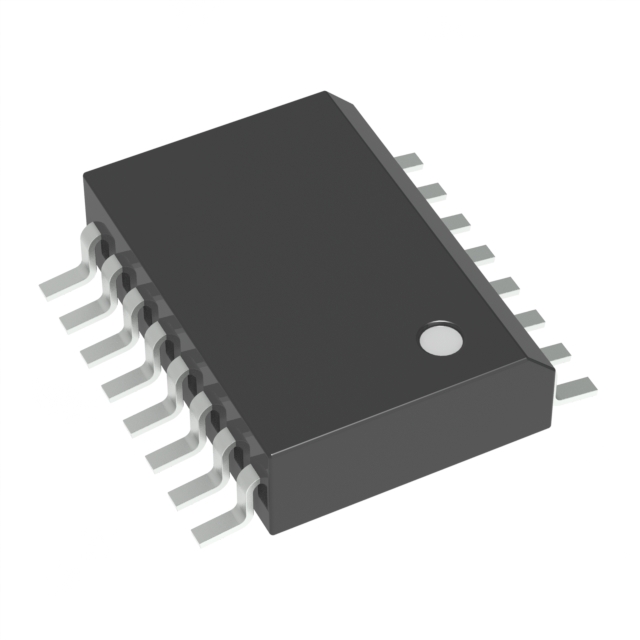
The SA571DR2G is supplied in a 16-pin SOIC-16 WB package. The device is Pb-free and is supplied in tape-and-reel packaging with 1,000 units per reel, making it suitable for automated SMT assembly.
-
Pin 1 - RECT CAP 1: connects the external averaging capacitor for the Channel 1 rectifier and controls gain-response timing.
-
Pin 2 - RECT IN 1: input to the Channel 1 full-wave rectifier used to detect average signal level.
-
Pin 3 - ΔG CELL IN 1: signal input to the Channel 1 variable-gain cell.
-
Pin 4 - GND: common ground connection for the device.
-
Pin 5 - INV. IN 1: inverting input of the Channel 1 operational amplifier.
-
Pin 6 - RES. R3 1: connection to the internal Channel 1 gain-setting resistor network.
-
Pin 7 - OUTPUT 1: processed analog output from Channel 1.
-
Pin 8 - THD TRIM 1: allows Channel 1 internal offset to be adjusted for lower distortion.
-
Pin 9 - THD TRIM 2: distortion-trim connection for Channel 2.
-
Pin 10 - OUTPUT 2: processed analog output from Channel 2.
-
Pin 11 - RES. R3 2: connection to the internal Channel 2 gain-setting resistor network.
-
Pin 12 - INV. IN 2: inverting input of the Channel 2 operational amplifier.
-
Pin 13 - VCC: positive power-supply input.
-
Pin 14 - ΔG CELL IN 2: signal input to the Channel 2 variable-gain cell.
-
Pin 15 - RECT IN 2: Channel 2 full-wave rectifier input.
-
Pin 16 - RECT CAP 2: Channel 2 external rectifier averaging-capacitor connection.
For SA571DR2G pinout design, the rectifier capacitors and external gain-setting components should be placed close to the related pins. The PCB should use a clean analog ground, short signal paths, and local power-supply bypassing. High-current switching traces, clock lines, and noisy digital buses should be kept away from the rectifier and variable-gain cell signal paths.
Key Features
-
Dual compressor and expander channels: either channel can be configured as a dynamic-range compressor or expander, allowing a complete companding system to be built for radio, telephone, modem, and audio applications using one IC.
-
Greater than 110 dB dynamic range: enables the circuit to process both weak and strong analog signals, helping improve usable signal range in communication and noise-reduction systems.
-
Temperature-compensated variable-gain architecture: reduces changes in gain behavior with temperature and improves consistency in equipment operating across changing environmental conditions.
-
Adjustable system levels: external components allow engineers to control gain, compressor or expander behavior, rectifier response time, and operating signal levels for different system requirements.
-
THD trimming capability: internal offset can be trimmed to reduce even-order harmonic distortion, providing additional value in audio and high-quality analog signal-processing designs.
-
Integrated voltage-controlled amplifier function: the variable-gain cell can be used for automatic gain control, dynamic filters, limiters, and other amplitude-control applications beyond conventional companding.
-
Low-voltage operation down to 6 V: allows the device to be integrated into compact communication and audio systems without requiring a high-voltage analog supply.
Applications
```

Cellular and Radio Communication
Use scenario: cellular radio, two-way radio, wireless voice links, and other analog radio communication equipment.
IC role: SA571DR2G compresses signal dynamic range before transmission and can expand the signal after reception.
Value: companding helps make better use of the available communication-channel dynamic range and can improve effective signal-to-noise performance.
|

Modem and Telephone Systems
Use scenario: analog modems, telephone interfaces, voice channels, and communication equipment with limited signal headroom.
IC role: the internal rectifier detects average signal amplitude while the variable-gain cell adjusts signal level according to the compressor or expander configuration.
Value: controlled dynamic-range processing helps maintain useful low-level information while reducing the risk of high-level signals exceeding the available channel range.
|

Noise Gate and Low-Level Expander
Use scenario: audio equipment, microphones, communication receivers, recording circuits, and systems requiring low-level noise suppression.
IC role: SA571DR2G reduces gain when the detected signal level falls below the intended operating range.
Value: background hiss and unwanted low-level noise can be reduced during quiet signal periods without continuously attenuating stronger wanted signals.
|

Dynamic Filter and High-Level Limiter
Use scenario: dynamic audio filters, level-sensitive signal processors, communication transmitters, and analog protection circuits.
IC role: the internal rectifier and variable-gain cell automatically adjust gain according to instantaneous or averaged signal amplitude.
Value: the circuit can limit excessive signal levels or dynamically alter filter behavior without requiring a complex external gain-control subsystem.
|
```
Equivalent & Alternatives
Engineers searching for an SA571DR2G equivalent should compare supply range, compressor and expander architecture, dynamic range, distortion, package, external timing components, pinout, and PCB compatibility. A device with similar compandor functionality should not automatically be treated as a direct drop-in replacement.
```
SA571DR2G vs SA572DR2G
The SA572DR2G is another dual-channel compandor from onsemi supplied in a 16-pin wide-body SOIC package. However, its architecture is more programmable and its external control and timing implementation differ from the SA571 design.
Selection advice: compared with SA572DR2G, SA571DR2G is better suited to designs already based on the established SA571 compressor, expander, rectifier, and internal operational-amplifier configuration. SA572DR2G can be considered where a new design can accommodate different external circuitry and programmable analog behavior.
SA571DR2G vs SA575DTBR2G
The SA575DTBR2G is a low-voltage compandor intended for applications requiring operation from lower supply voltages. It uses a different package and internal architecture from SA571DR2G.
Selection advice: choose SA571DR2G when the design uses a 6 V to 18 V supply and requires the SA571 dual gain-control architecture. SA575DTBR2G may be more appropriate for lower-voltage portable equipment, but it requires circuit and PCB redesign rather than direct substitution.
```
Quality & Handling
SA571DR2G should be sourced as an original onsemi component through controlled and traceable supply channels. Because analog compandor performance depends on gain accuracy, distortion, noise, and stable biasing, incoming inspection is especially important for production applications.
-
Original component verification: verify manufacturer marking, SA571DR2G part number, lot information, date code, packaging, and supplier documentation.
-
Incoming inspection: inspect package condition, lead integrity, reel labeling, moisture exposure, and physical consistency before PCB assembly.
-
Electrical testing: critical applications can verify supply current, gain behavior, channel separation, distortion, and compressor or expander transfer characteristics.
-
ESD handling: use grounded ESD-safe workstations, antistatic packaging, and suitable operator protection throughout storage and assembly.
-
Traceability: maintain supplier, lot, date-code, inspection, and shipment records for quality-control and failure-analysis purposes.
Availability & Supply Support
SA571DR2G is a Pb-free tape-and-reel version of the SA571 family supplied in a 16-pin SOIC package. Tape-and-reel packaging supports automated SMT manufacturing and volume production.
For stable supply, buyers should confirm current manufacturer status, distributor inventory, date code, lead time, reel quantity, and traceability before placing production orders.
For long-term programs, forecast-based procurement, scheduled deliveries, and approved alternative-source planning can help reduce supply risk. This is particularly useful in communication, industrial, professional audio, and legacy-equipment programs where the same compandor may be required across multiple production cycles.
Manufacturer
onsemi is a global semiconductor manufacturer serving automotive, industrial, communications, power-management, sensing, analog, mixed-signal, and embedded-electronics markets. Its portfolio includes analog signal-conditioning devices, amplifiers, interfaces, power semiconductors, sensors, and other components used in electronic systems.
The SA571DR2G reflects onsemi's established analog signal-processing technology by integrating dual rectifiers, temperature-compensated variable-gain cells, operational amplifiers, and adjustable external timing networks into one device. This architecture allows engineers to implement dynamic-range control with fewer external active components.
FAQ
```
What is the SA571DR2G?
SA571DR2G is a dual-channel compandor IC from onsemi. Each channel contains a full-wave rectifier, temperature-compensated variable-gain cell, and operational amplifier and can be configured for compression, expansion, noise reduction, limiting, dynamic filtering, or voltage-controlled amplification.
Where can I find the SA571DR2G datasheet download?
The official SA571DR2G datasheet download is available from onsemi under the SA571 product documentation. The SA571DR2G datasheet includes electrical characteristics, internal block diagrams, SA571DR2G pinout information, compressor and expander circuits, design equations, package dimensions, and ordering information.
What should engineers consider for SA571DR2G pinout design?
For SA571DR2G pinout design, keep the rectifier capacitors, gain-setting resistors, and signal-path components close to the IC. Use clean analog grounding, local VCC decoupling, and adequate separation from switching regulators, clocks, high-current traces, and digital buses.
What is a typical SA571DR2G application?
A typical SA571DR2G application is a communication companding system where a wide-dynamic-range analog signal is compressed before transmission and expanded after reception. Other applications include cellular radio, modems, telephone equipment, noise gates, high-level limiters, dynamic filters, and voltage-controlled amplifiers.
What is the SA571DR2G equivalent?
There is no universal drop-in SA571DR2G equivalent. SA572DR2G and SA575DTBR2G are possible functional alternatives for some compandor applications, but their architectures, packages, supply requirements, and external circuits differ. PCB and circuit redesign may therefore be required.
SA571DR2G vs SA572DR2G: what is the difference?
In an SA571DR2G vs SA572DR2G comparison, both devices provide analog compandor functions, but SA572DR2G uses a different programmable architecture and different external circuit requirements. SA571DR2G is normally the better choice for existing SA571-based designs, while SA572DR2G may be considered for new circuits designed around its architecture.
What supply voltage does SA571DR2G require?
SA571DR2G operates from approximately 6 V to 18 V. The latest manufacturer datasheet should be used to confirm operating conditions, electrical limits, and external component values before completing the power-supply design.
How does SA571DR2G control gain?
The internal full-wave rectifier detects the average input-signal level and charges an external rectifier capacitor. The resulting control signal determines the gain of the temperature-compensated variable-gain cell, allowing gain to follow changes in signal amplitude.
How does the rectifier capacitor affect SA571DR2G performance?
A smaller rectifier capacitor produces faster gain response but allows more low-frequency ripple in the gain-control signal. A larger capacitor provides smoother control but slower attack and decay. The capacitor value should therefore be selected according to the frequency content and response requirements of the application.
```